Sustainable PCB Layout: Considerations for High Frequency DesignsAuthor : Adrian October 07,how to choose solder paste 2025Table of ContentsIn the fast-paced world of electronics, designing high-frequency PCBs (Printed Circuit Boards) requires precision and a deep understanding of signal behavior. But how can you create layouts that not only perform well at high frequencies but also embrace sustainability? This blog dives into the key considerations for high-frequency PCB design, focusing on impedance control, signal integrity, dielectric materials, and stack-up design, all while integrating sustainable practices to reduce environmental impact. Whether you're an engineer working on cutting-edge 5G applications or designing high-speed digital circuits, this guide will walk you through actionable strategies to optimize your PCB layouts. Let’s explore how to balance performance with eco-friendly design choices for a greener future in electronics.
Why Sustainable High-Frequency PCB Design MattersHigh-frequency PCB design is critical for applications like telecommunications, automotive radar, and IoT devices, where signals operate at frequencies above 1 GHz. At these speeds, even small layout errors can lead to signal loss, interference, or complete failure. Meanwhile, sustainability in electronics is no longer just a trend—it’s a necessity. The industry is under pressure to minimize waste, reduce energy consumption, and use eco-friendly materials without compromising performance. By combining sustainable practices with high-frequency design principles, you can create PCBs that meet modern performance demands while contributing to a healthier planet. Let’s break down the core elements of this approach.
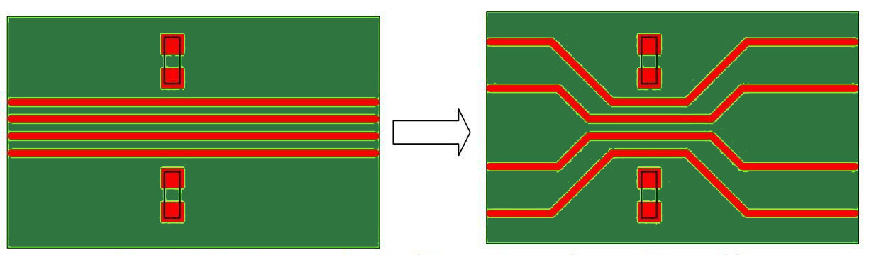
Key Considerations for High-Frequency PCB DesignDesigning for high frequencies involves tackling challenges like signal degradation, electromagnetic interference (EMI), and impedance mismatches. Below are the critical factors to consider, paired with sustainable strategies to enhance your layout process. 1. Impedance Control: The Backbone of Signal PerformanceImpedance control is essential in high-frequency PCB design to ensure signals travel without distortion. Mismatched impedance can cause reflections, leading to data errors or signal loss. For example, a common target impedance for high-speed digital signals is 50 ohms, often used in USB or Ethernet applications. To achieve proper impedance control:
2. Signal Integrity: Ensuring Clean Data TransmissionSignal integrity refers to the quality of an electrical signal as it travels through the PCB. At high frequencies, issues like crosstalk, noise, and timing errors become more pronounced. Poor signal integrity can result in bit errors or system failures, especially in applications like 5G or high-speed computing. Here are practical tips to maintain signal integrity:
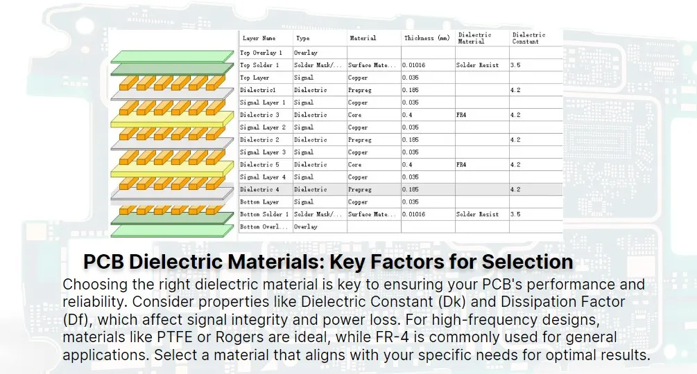
3. Dielectric Materials: Choosing the Right FoundationThe choice of dielectric material significantly impacts high-frequency performance. Dielectric constant (Dk) and dissipation factor (Df) determine how signals propagate through the board. Materials with a lower Dk allow faster signal speeds, while a low Df reduces signal loss. For high-frequency designs, consider these material properties:
Selecting the right dielectric material is a balancing act between performance, cost, and sustainability. Always evaluate the specific frequency requirements of your project before deciding.
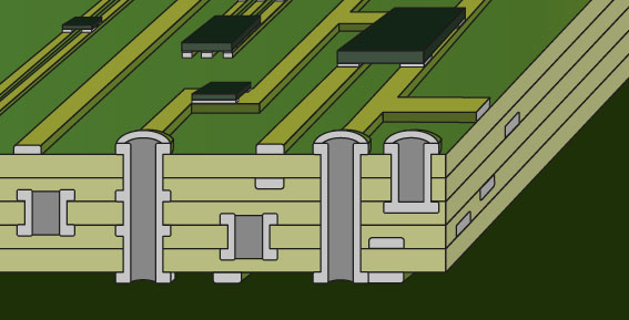
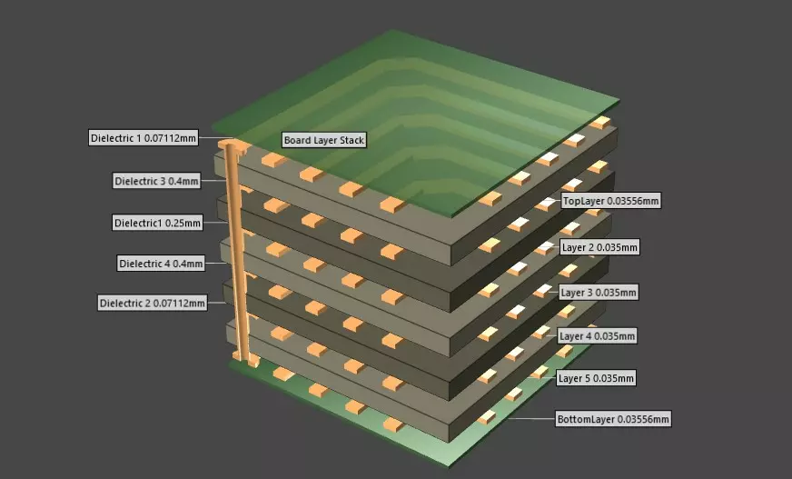
4. Stack-Up Design: Building a Solid StructurePCB stack-up design defines the arrangement of signal, ground, and power layers in a multilayer board. A well-planned stack-up is crucial for managing signal integrity, EMI, and thermal performance in high-frequency designs. Key principles for effective stack-up design include:
A carefully designed stack-up not only boosts signal performance but also contributes to a more sustainable manufacturing process by reducing waste.
Sustainability in High-Frequency PCB LayoutSustainability is a growing priority in electronics design. By integrating eco-friendly practices into high-frequency PCB layouts, you can reduce environmental impact while maintaining top-tier performance. Here are some actionable ways to make your designs greener. 1. Material Selection for a Greener FutureChoosing sustainable materials is a powerful step toward reducing the environmental footprint of PCB production. Focus on:
2. Efficient Design to Minimize WasteEfficient PCB layouts can significantly cut down on material waste during production. Consider these strategies:
3. Energy-Efficient PerformanceHigh-frequency PCBs often power energy-intensive applications. Designing for energy efficiency benefits both performance and sustainability:
Challenges in High-Frequency PCB Design and Sustainable SolutionsHigh-frequency designs come with unique challenges that can complicate sustainability efforts. However, with the right approach, these hurdles can be overcome. Challenge 1: Signal Loss at High Frequencies Challenge 2: EMI and Shielding Needs Challenge 3: Manufacturing Complexity
Best Practices for Balancing Performance and SustainabilityTo wrap up, here are some best practices to ensure your high-frequency PCB designs excel in both performance and sustainability:
Conclusion: Designing for the FutureHigh-frequency PCB design is a complex field that demands attention to impedance control, signal integrity, dielectric materials, and stack-up design. By weaving sustainability into these considerations, you can create layouts that not only meet the rigorous demands of modern electronics but also contribute to a more environmentally conscious industry. From selecting low-loss, eco-friendly materials to optimizing trace routing for minimal waste, every decision in the design process counts. As technology continues to evolve, embracing sustainable practices in PCB layout will ensure that high-frequency designs remain innovative and responsible. With these strategies, you’re well-equipped to build PCBs that power the future—both in performance and sustainability. Share · · · · The Role of Flux in PCB Wave Soldering: Selection, Application, and Residue RemovalMarch 16, 2026PCB wave soldering flux types include rosin, water-soluble, and no-clean options with varying activity levels for oxide removal and solder flow. This guide covers selection criteria, spray foam drop-jet application methods, residue removal processes, and alternatives like nitrogen blanketing to boost joint reliability and yields for engineers. Article Achieving Uniform Solder Fillets in PCB Wave Soldering: Process ControlMarch 16, 2026Achieve uniform solder fillets in PCB wave soldering with process control strategies. Optimize flux, preheat, wave height, conveyor speed for consistent fillet shape, height, and wetting balance. Includes visual inspection tips and troubleshooting for reliable through-hole assemblies. Boost quality in production. Article Optimizing Conveyor Speed for Efficient PCB Wave SolderingMarch 16, 2026Learn PCB wave soldering conveyor speed calculation to manage dwell time, immersion depth, and throughput effectively. Electric engineers get practical steps, best practices, and troubleshooting tips for higher process efficiency and fewer defects in wave soldering operations. Article Understanding IPC Standards for PCB Surface Finishes: Ensuring Quality and ComplianceMarch 11, 2026Understand IPC standards IPC 4552 ENIG and IPC 4553 immersion silver for PCB surface finishes. Ensure compliance, enhance solderability, and prevent common defects to achieve reliable, high quality circuit boards. Article Miniaturization Challenges in PCB AssemblyMarch 11, 2026Navigate the complexities of high density interconnect PCB assembly and precise component placement. Learn to tackle miniaturization challenges, from tiny part handling to thermal stress, ensuring robust and reliable electronics. Article High Speed Routing Techniques: PCBMarch 11, 2026Master high speed routing in PCBs to ensure signal integrity and minimize electromagnetic interference. Learn essential techniques for robust designs, from controlled impedance to differential pair strategies. Prevent performance issues and achieve reliable electronics. ArticleGet Instant PCB |